
As deep learning models scale into trillions of parameters, software optimization is hitting a hard physical wall. In mid-2026, the tech industry has reached a consensus: the next leap in AI capabilities will not come from algorithms alone, but from the raw silicon beneath them. We are witnessing a twin-engine revolution: the launch of highly customized AI inference silicon, exemplified by OpenAI's custom chip "Jalapeño", and the historical engineering breakthrough of sub-1nm node chip architectures.
This article dives into how these hardware breakthroughs are redefining the economics of intelligence, bypassing the limits of physics, and shifting the global geopolitical landscape of computing power.
1. The Physical Wall: Why Software Optimization is No Longer Enough
For the past decade, AI scaling relied heavily on general-purpose Graphics Processing Units (GPUs) designed originally for parallel graphics rendering. However, Large Language Models (LLMs) and agentic workflows create a completely different computational workload. They are heavily bound by memory bandwidth (the speed at which weights are transferred from memory to processing cores) rather than raw compute cycles.
As memory bottlenecks translate to high latencies and astronomical electricity costs, the industry is shifting away from generalized computing toward domain-specific architectures—chips designed from the ground up to do exactly one thing: execute AI models at the lowest possible cost per token.
2. OpenAI's 'Jalapeño': The Rise of Dedicated Inference Silicon
The unveiling of OpenAI's first custom-designed inference chip, Jalapeño, represents a major structural shift in the AI value chain. Co-developed with Broadcom and manufactured on TSMC's advanced process nodes, Jalapeño is an Application-Specific Integrated Circuit (ASIC) built specifically for transformer-based inference.
Low-latency Memory and On-Chip Interconnects: Jalapeño bypasses standard memory hierarchies by integrating massive amounts of high-bandwidth memory (HBM) directly adjacent to the processing cores, coupled with ultra-fast interconnects. By keeping active weights on-chip, Jalapeño reduces the energy required to retrieve data, leading to a massive drop in operating costs and enabling true, real-time conversational and reasoning capabilities at scale.
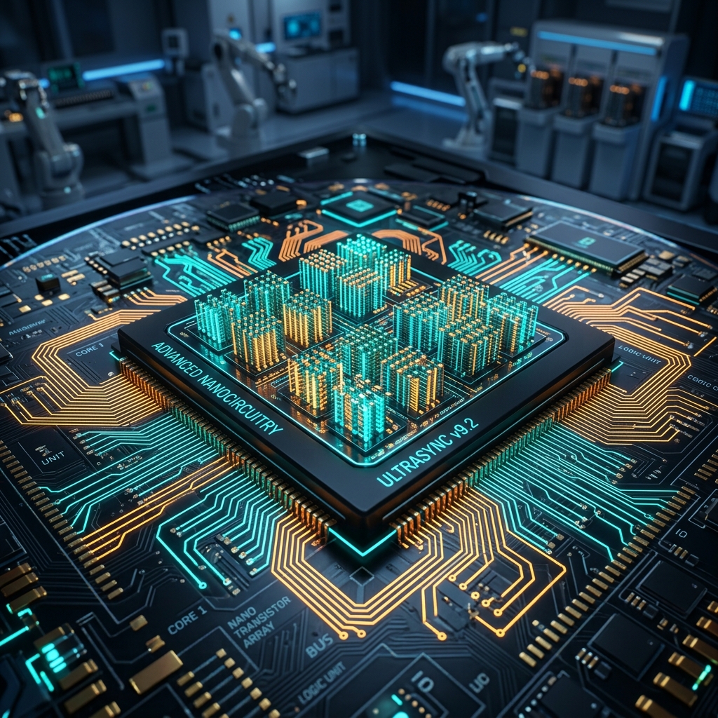
3. IBM's Sub-1nm Milestone: Bypassing Silicon Scaling Limits
While OpenAI tackles specialized chip architectures, materials science is breaking fundamental physical limits. IBM Research recently announced the fabrication of the world's first working sub-1nm (0.7-nanometer / 7 angstrom) transistor node.
For years, experts warned that silicon transistors could not shrink below 1nm due to quantum tunneling—a phenomenon where electrons leak through barriers that are too thin. IBM bypassed this scaling limit by employing a 3D "nanostack" nanosheet architecture. By stacking three or four nanosheet channels vertically, they maximize current flow and gate control in a microscopic footprint, promising a 45% performance boost or a 75% reduction in energy usage compared to current leading-edge 2nm nodes.
4. Hardware Acceleration for Agentic AI and Embodied Robotics
The primary beneficiary of these hardware leaps is the field of Agentic and Physical AI. Autonomous agents must continually loop through a cycle of observation, reasoning, tool selection, and action. If each step of this loop takes seconds due to cloud server latency, the agent becomes sluggish and impractical for real-world tasks.
With high-performance, energy-efficient chips like Jalapeño and sub-1nm silicon, we can host smaller, highly compressed reasoning models locally on edge devices, drones, and humanoid robots. This local, near-zero-latency execution is the missing link needed to make embodied AI reactive, safe, and truly autonomous in complex, dynamic environments.
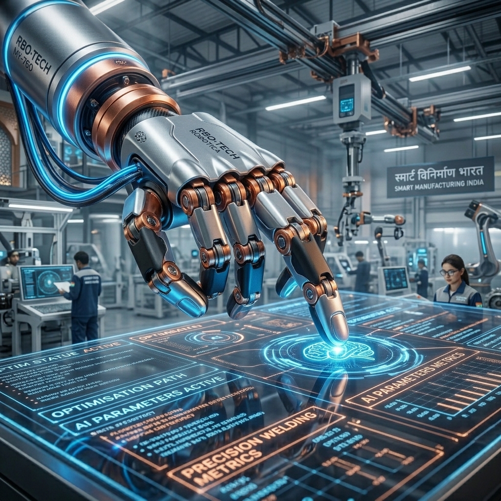
5. The Geopolitics of Semiconductors and India's Position
The race for next-generation silicon has become the central front of global technology geopolitics. Advanced chip manufacturing requires extreme capital expenditures and relies on a highly consolidated supply chain involving ASML (lithography), TSMC (foundry), and global design firms.
In India, the momentum is growing rapidly. Boosted by the India Semiconductor Mission (ISM) and capital inflows like Amazon's massive $13 billion infrastructure expansion, the nation is building out assembly, testing, and packaging (OSAT) facilities. By integrating design capabilities with manufacturing partnerships, India is positioning itself as a resilient alternative node in the global deep-tech supply chain, securing the compute power needed for its domestic digital economy.
6. Overcoming Manufacturing and Cooling Bottlenecks
Scaling chips down to the angstrom level introduces unprecedented engineering challenges, particularly regarding lithography and thermal management:
- High-NA EUV Lithography: Printing patterns at a sub-1nm scale requires ASML's High-NA Extreme Ultraviolet lithography machines. These massive systems use larger numerical apertures to focus light to a finer resolution, demanding extreme alignment precision down to a few picometers.
- Thermal Management: As transistors pack closer together, the heat density surges. Conventional air cooling is completely inadequate. Companies are turning to liquid immersion cooling and direct-to-chip microfluidic systems, routing coolant directly over the back of the silicon to prevent thermal throttling.
7. The Outlook: The Post-Silicon Future
While the sub-1nm milestone extends the life of traditional semiconductor architectures, we are approaching the absolute physical limit of silicon. The next decade will likely force a transition to alternative channel materials like carbon nanotubes, two-dimensional transition metal dichalcogenides (TMDs), or fully optical computing architectures.
In the near term, the combination of customized AI ASICs and 3D-nanostack silicon will provide more than enough computational headroom to scale the global intelligence grid, making intelligence so cheap and abundant that it becomes utility-like.
Conclusion
The chip revolution of 2026 reminds us that the virtual world of artificial intelligence is fundamentally tethered to the physical world of silicon, atoms, and electricity. Whether it is custom inference silicon like OpenAI's Jalapeño or the sub-1nm nanosheets forged in fabrication labs, the hardware layer remains the ultimate foundation of the digital future. The race is no longer just about writing code; it is about writing it in the very structure of matter.